

I finished my bachelor’s degree in Electrical Engineering, Telecommunication, from Azad University, Mashhad Branch, Iran. In 2012, I successfully achieved the 174th rank (out of more than 10000 electrical engineering applicants) through an extremely competitive national university entrance exam, and I won a scholarship for the Master’s program at the University of Tehran, the most prestigious university in Iran. I joined the Electronics department, known as the most advanced faculty in Nanoelectronics in Iran, and hosted lots of modern micro/nano-fabrication equipment and modern computing infrastructure for multiscale and multiphysics simulations.
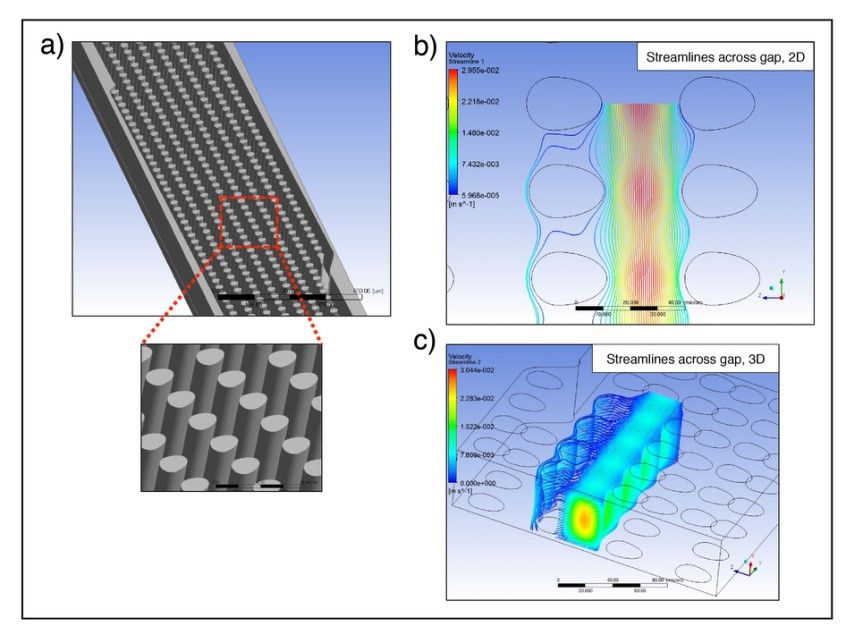
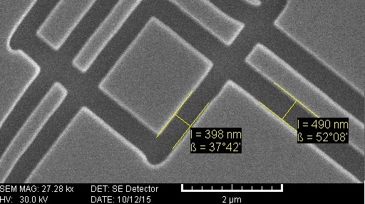
Studying for a master’s degree at the top-ranked university of Iran, opened up a new world to me, and I was motivated to improve my knowledge and prove myself even more. I started my thesis under the supervision of professor Fathipour who was the director of three comprehensive labs, including 1) TCAD Lab (Simulation), 2) MEMS & NEMS Lab (The most advanced nanolithography center in Iran), and 3) Nano Measurement Lab. All these helped me discover my research interest and clarify the steps I have taken. My master’s thesis was on bio-particle separation with dielectrophoresis (simulation and fabrication). I successfully designed a device that could be used to determine specific disease types by utilizing the Gaussian pattern of cell movements. Also, I have participated in plasmonic projects (Terahertz/Plasmonic photoconductive antenna” Fabricated by E.B.L”, LSPR/Plasmonic Gold Nano-Island ”Fabricated by Dr. Blade method”, etc.,) and my research resulted in two journal publications and three conferences.
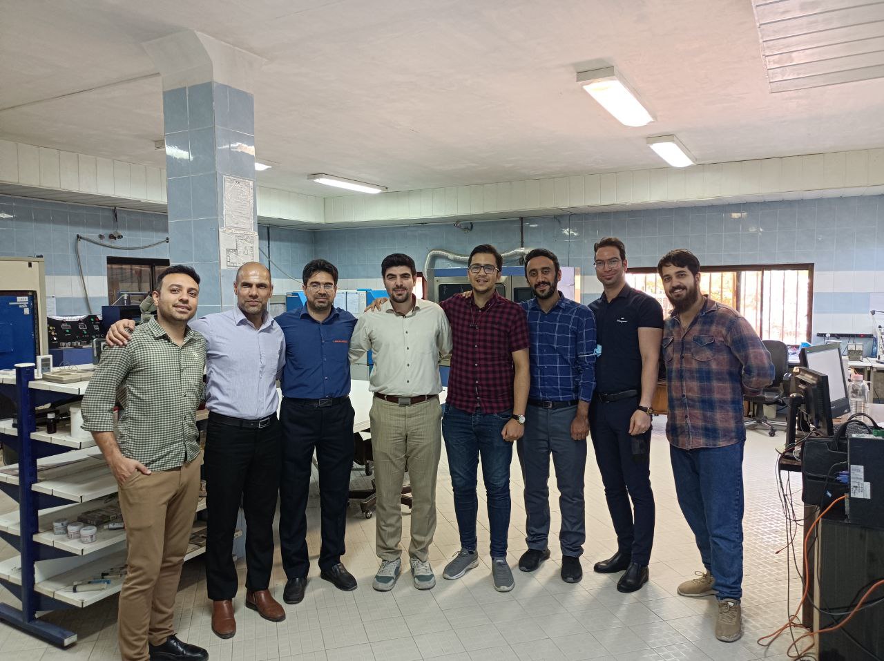
 During my master’s study, I participated in establishing the MEMS & NEMS lab (Cleanroom). When I started my thesis work, the cleanroom was in the early phase of building, so I had to initialize some new equipment or sometimes create equipment from scratch. Having graduated, I started my career as a cleanroom manager and researcher at the MEMS & NEMS Lab.

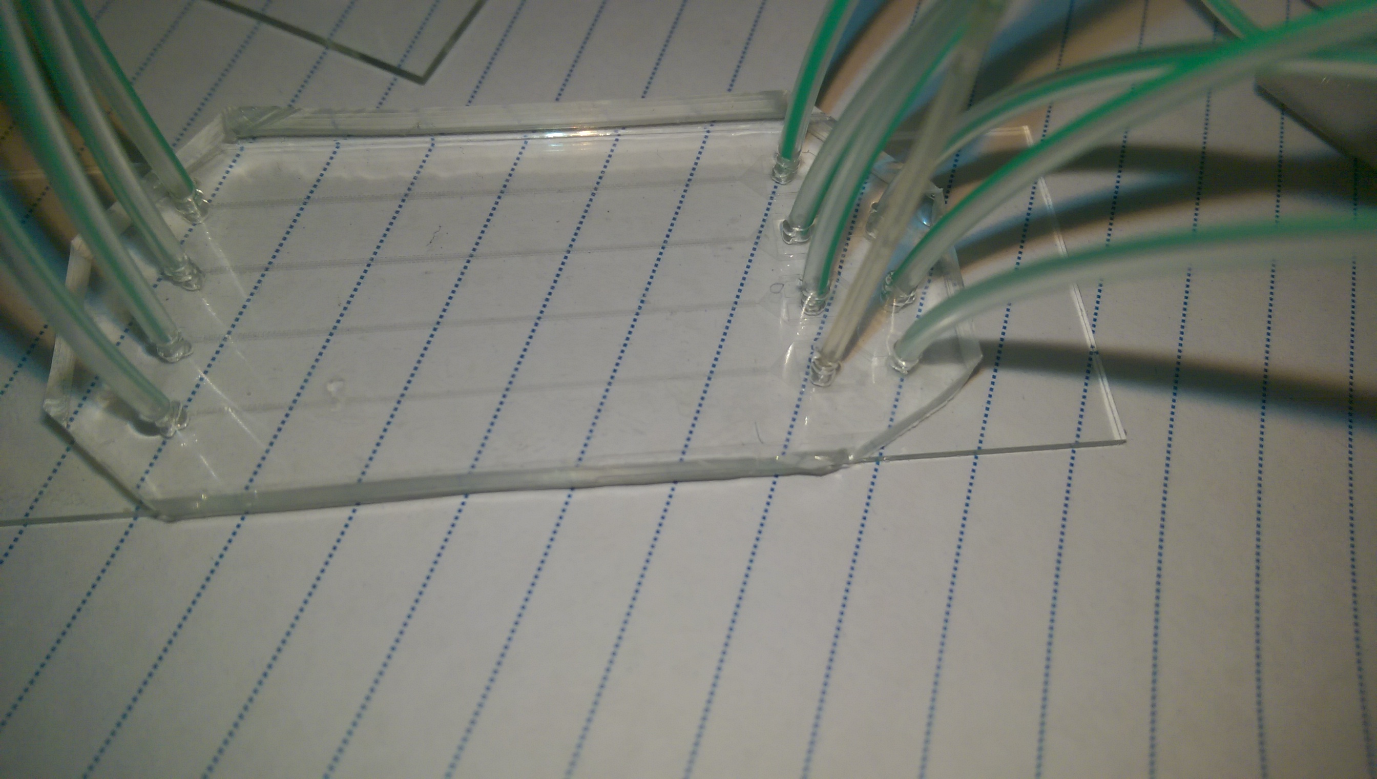
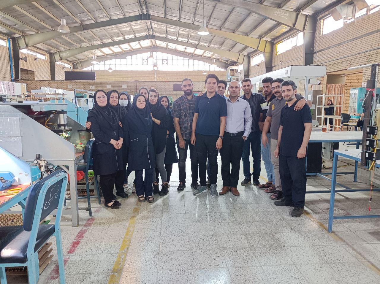
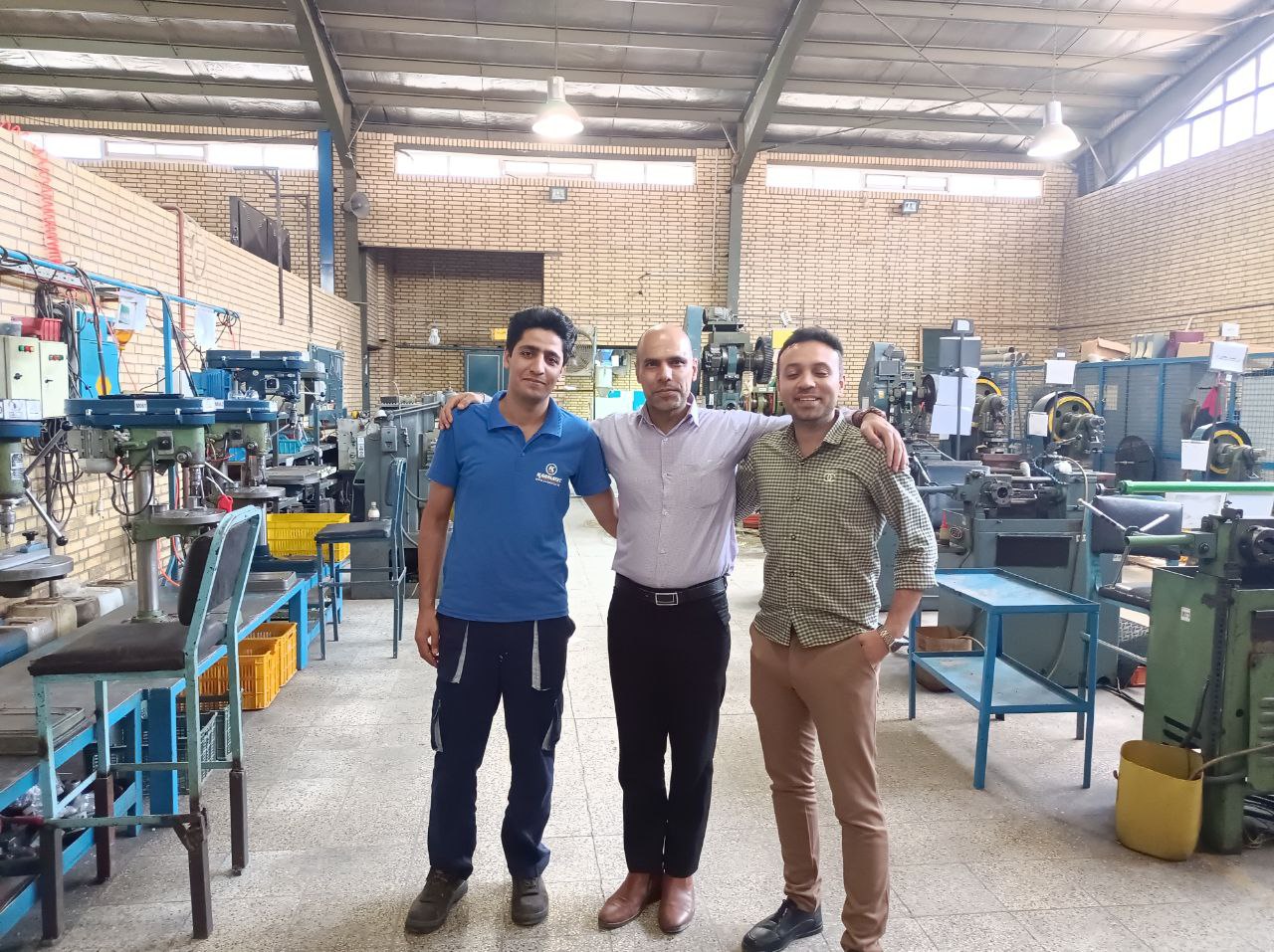
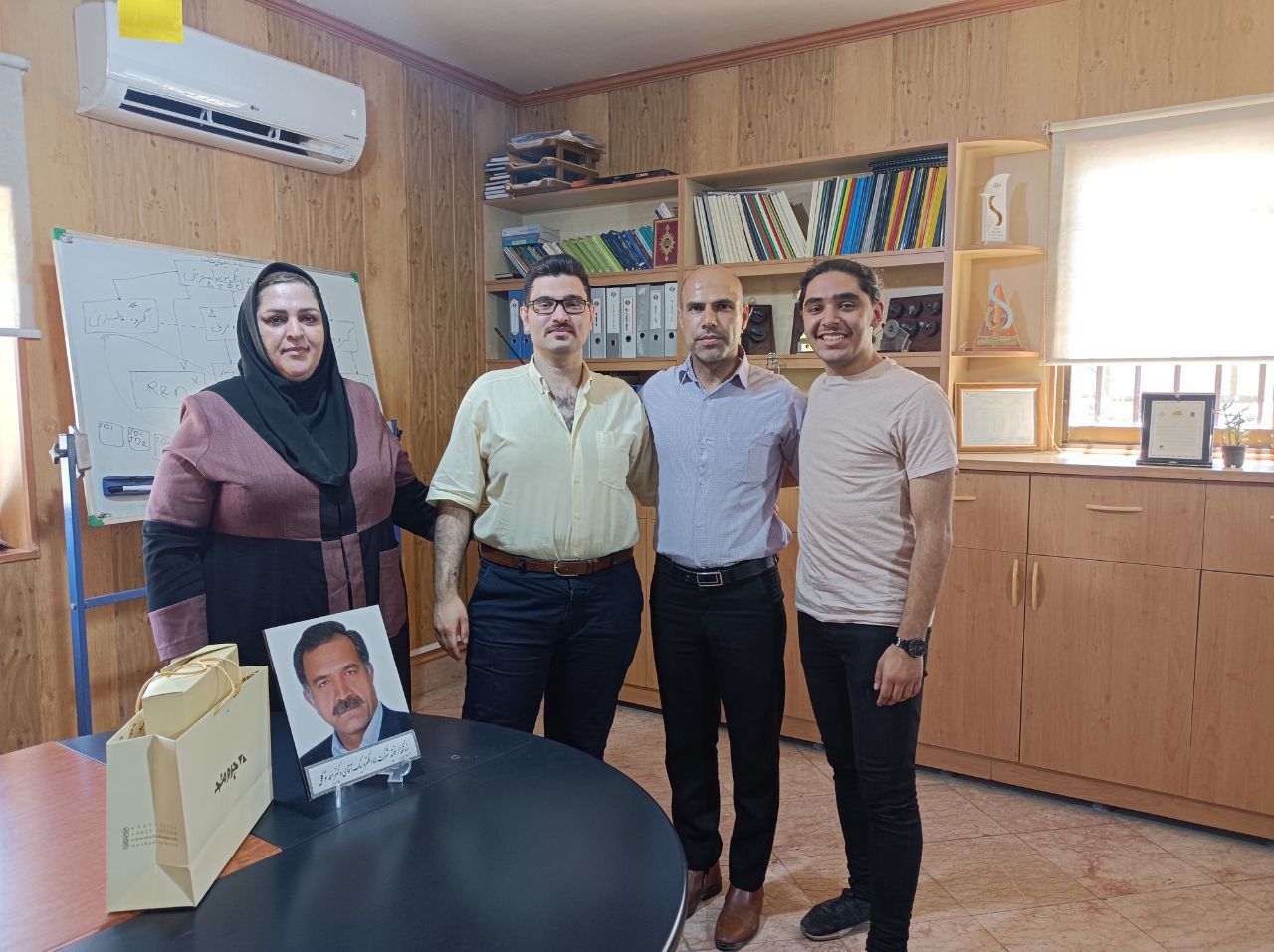
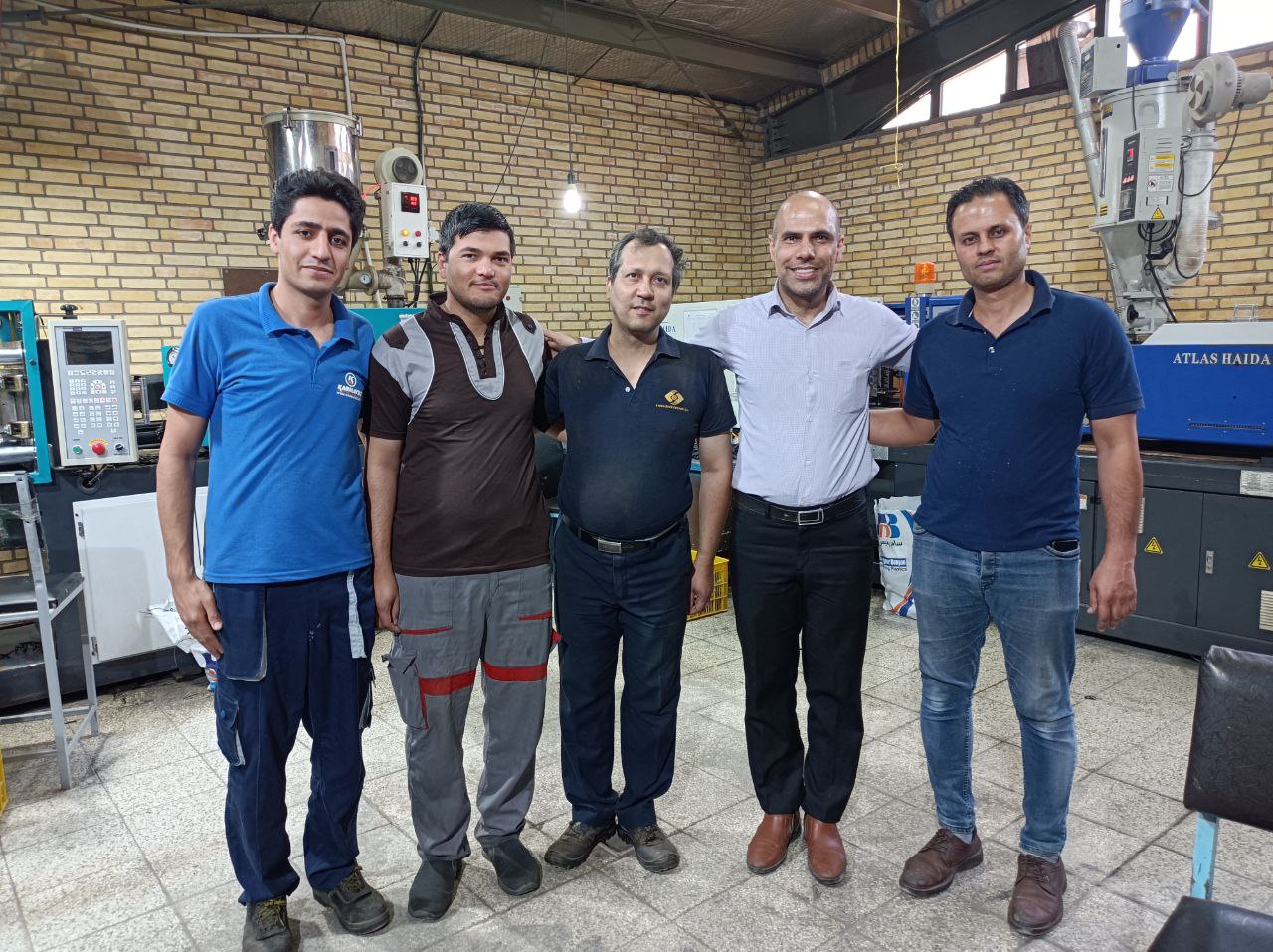
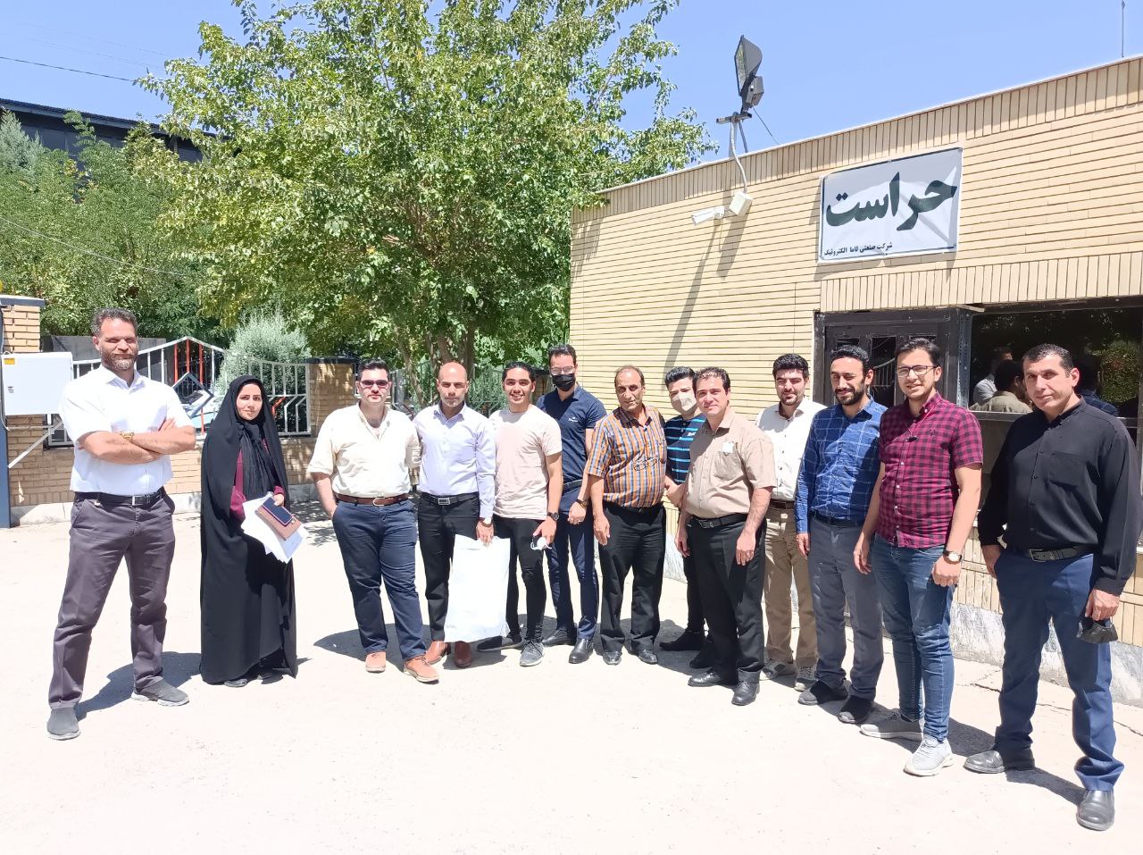
In 2019, I joined the R&D Department of LAMA Electronic company to conduct research on ceramic-based oxygen sensors. In all the years that I have worked as a nanotechnology researcher, I have participated in many research projects in order to design and fabricate biosensors and Lab On Chip(L.O.C). I usually use COMSOL Multiphysics to simulate the L.O.C/Biosensors ideas that can help develop functional structures. Furthermore, I have embraced fruitful experiences in the fabrication of Micro/Nano devices. What is more, by working in the LAMA electronics company, I learned how to design a product for mass production. In 2021 I joined Razavi High Tech Venture Capital as a Senior Venture Capital Analyst to analyze the Technical/Financial/Market aspects of startups and companies in the field of microelectronic and advanced medical devices. Being in the TCAD Lab and MEMS&NEMS Lab gave me the opportunity to learn about the design, fabrication, and analysis of biosensors, L.O.C and MEMS devices, and working in LAMA Electronic company gave me the chance to understand the real-life challenges in the production of sensors out of the academic areas. Joining Razavi VC was a milestone in my professional life; I learned how I should look at the future of scientific projects, manage sources, risks, team working, strategies, Etc. These items are not only related to the startups; these are in touch with every project and every step that we need to take to turn Dreams and Passions into Reality.
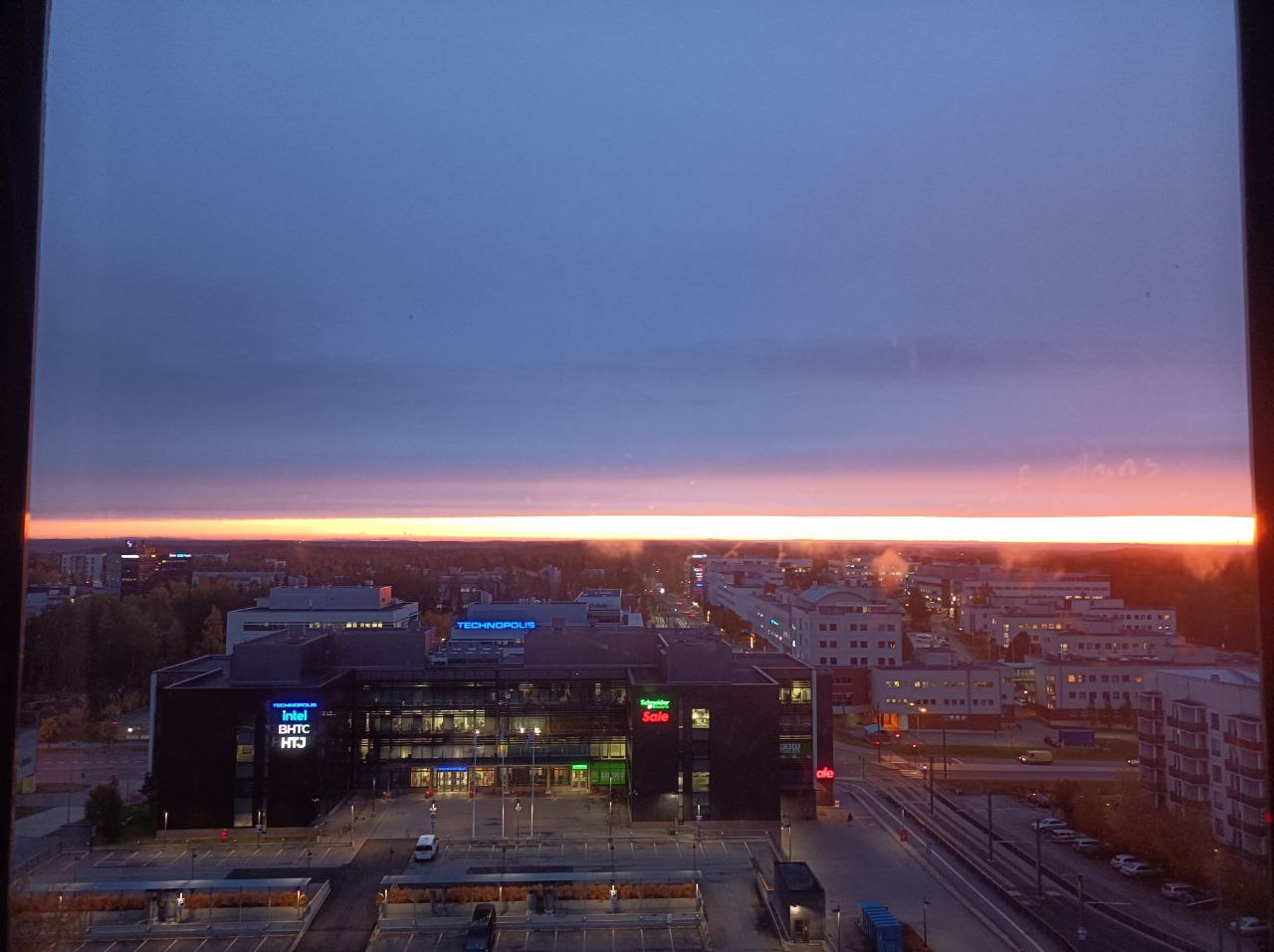
In Sep 2022, I moved to Tampere Finland and now I am more focused on Human-Technology-Interactions to learn more about designing applicable Lab-on-chip and nanotechnology devices.

I'm so passinate to design applicable and functional products specially in the field of Lab On Chip.
My skills can be classified into three sections: